
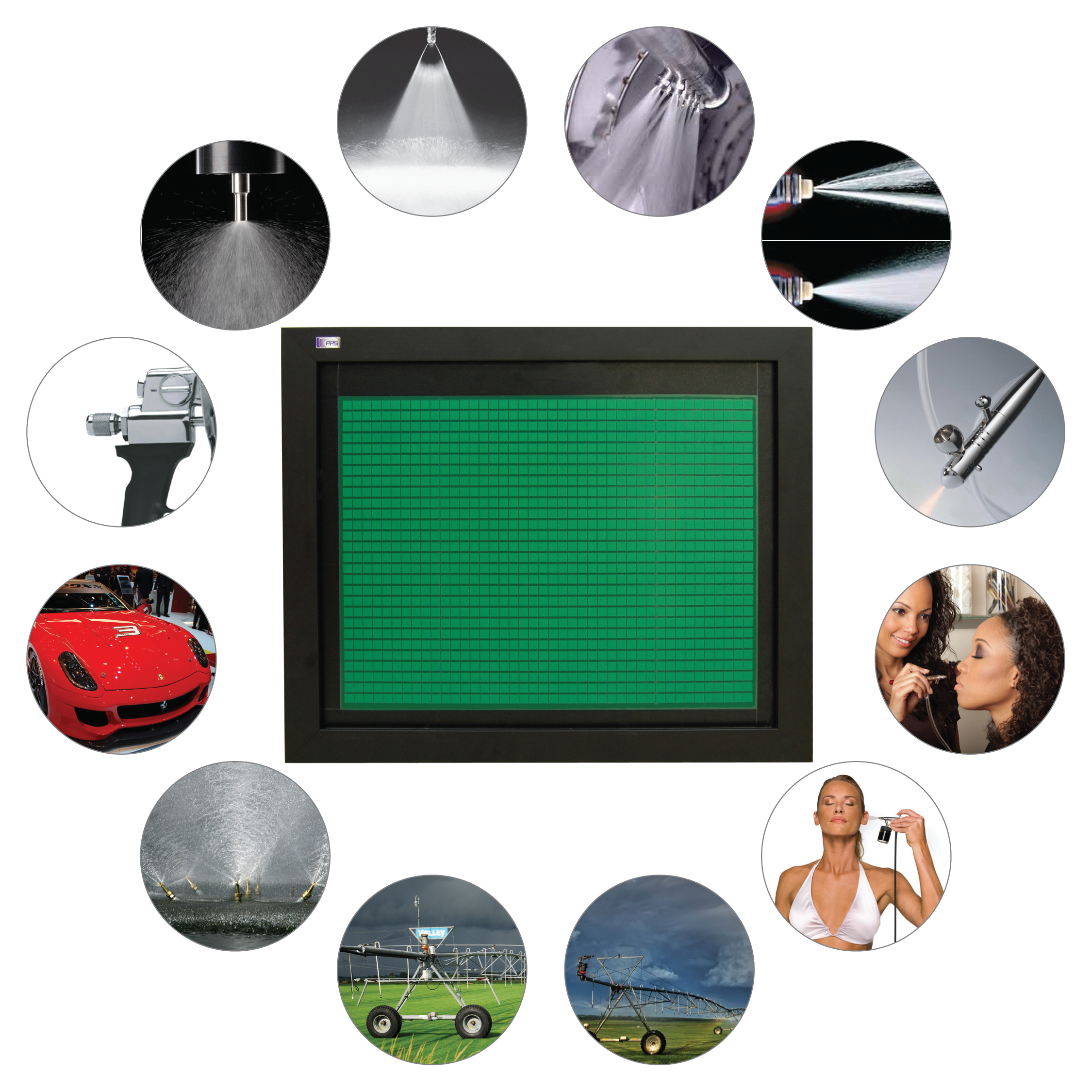
Applications for PPS sensors & Technology
PPS tactile pressure sensors measure contact forces and pressure distribution, turning physical interaction into usable data. Engineers, designers, and researchers use PPS systems to understand how forces behave in real-world conditions. PPS offers both pre-defined sensing solutions and custom options to support established applications as well as advanced R&D work.
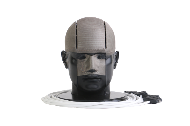
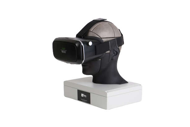
인체 접촉 압력 매핑
Quantify how pressure is distributed between the human body and support surfaces. This application is crucial for comfort and ergonomic assessment in product design, clinical evaluation, and wearable testing. PPS pressure mapping solutions deliver repeatable, high-resolution data that helps teams optimize cushioning, posture support, and fit for consumer goods, medical devices, and performance gear.

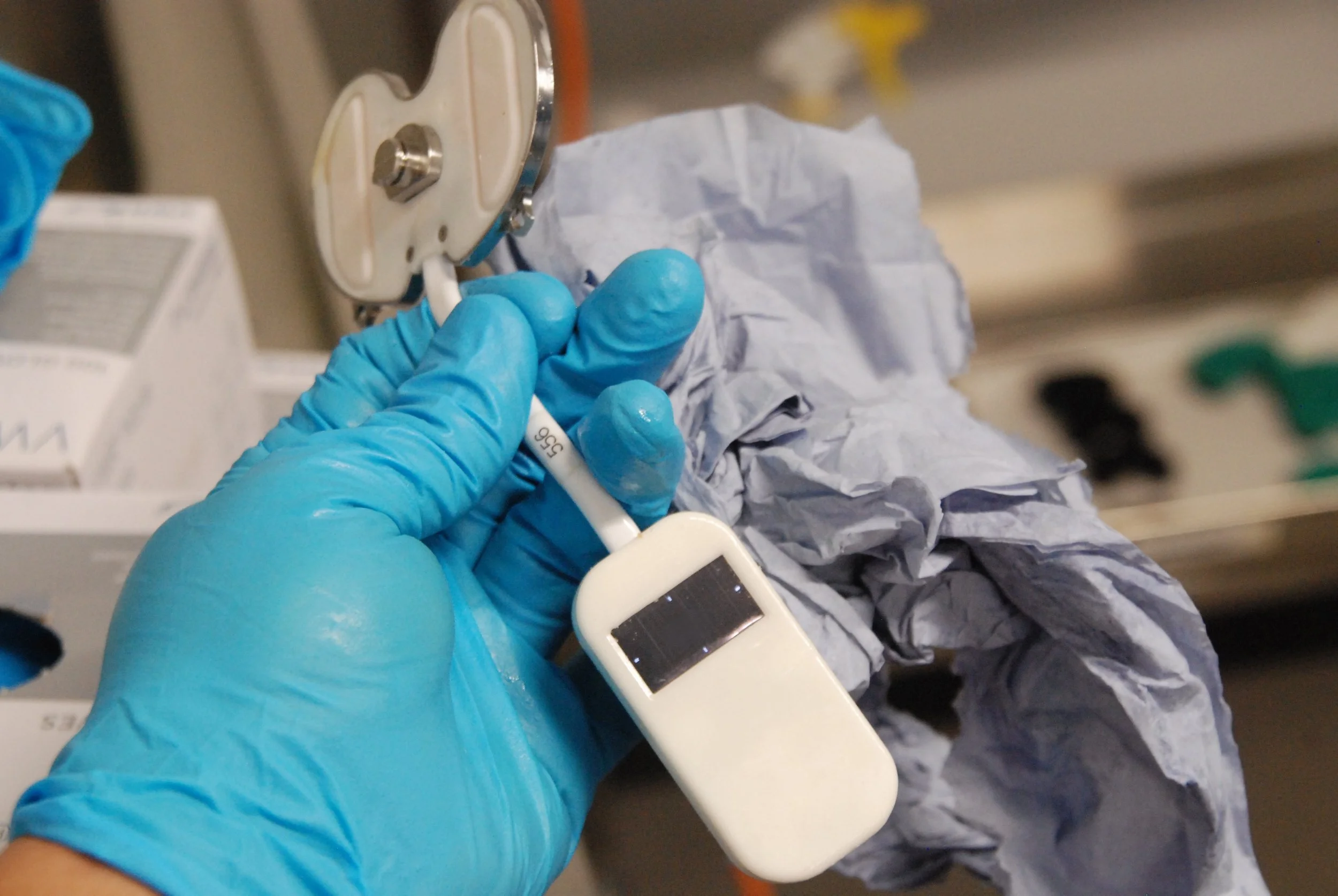
의료 기기
PPS는 지난 30년 동안 수많은 의료 프로젝에서 헌신적인 파트너로서 임해왔습니다. PPS의 특허 기술로 고객사의 혁신적인 아이디어를 올바로 반영하고 PPS만의 전문 생산기술로 모두가 만족하는 합리적인 비즈니스가 될 수 있도록 도와 드리겠습니다.
반도체 산업용
Our tactile sensing technology has allowed semiconductor manufacturers to improve tolerances in manufacturing and produce wafers with more precision and accuracy. This application of low-pressure sensors has fuelled products that optimize semiconductor polishing disk pressures while significantly reducing tilt errors. The ultra-low-pressure sensitivity of the 스프레이(Spray) allows for precision measurement, testing, and refinement of cleaning sprays, aerosol nozzles, and any other application involving low pressure or pattern distribution.
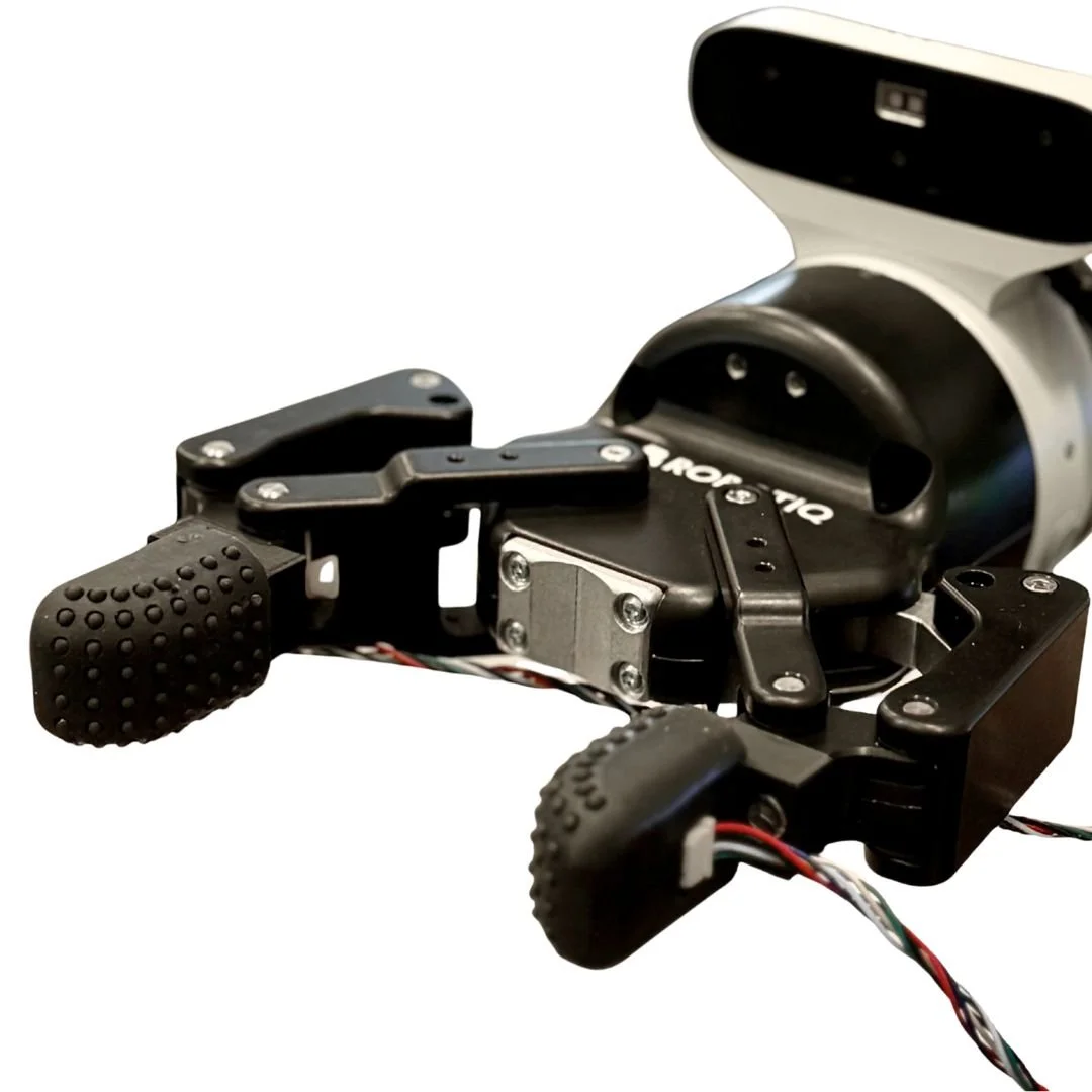
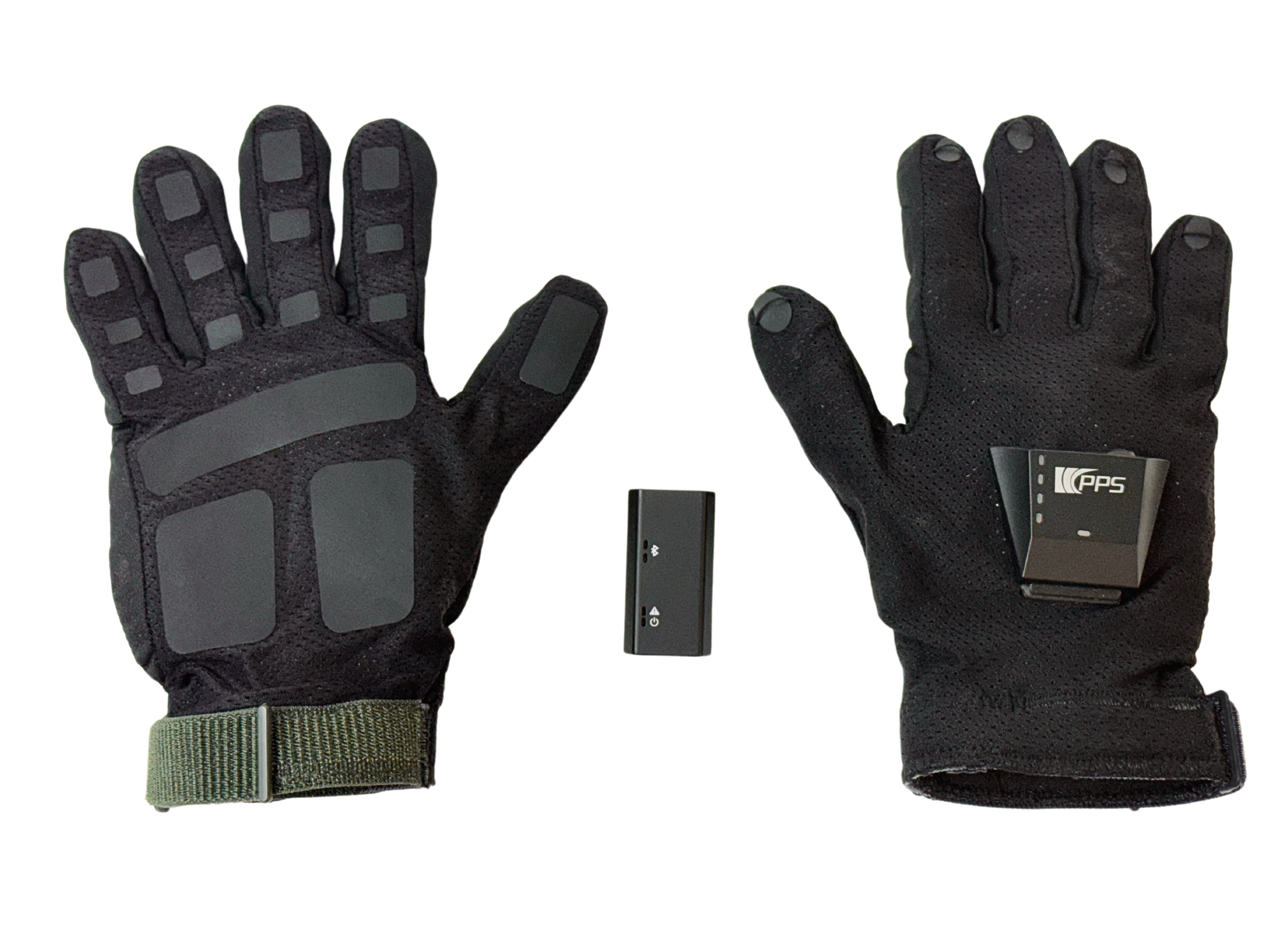
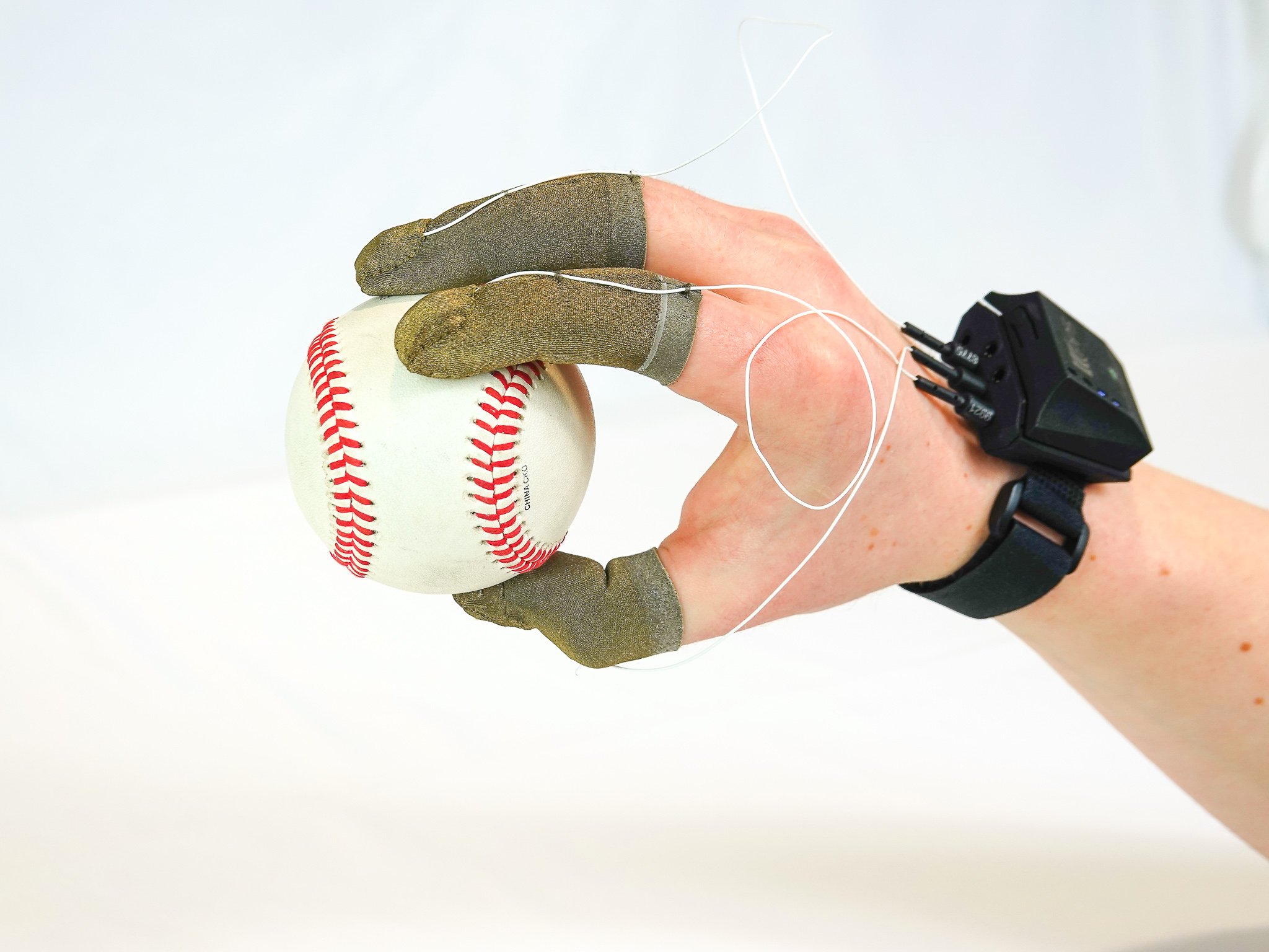
Robotics — Enabling Sense of Touch
PPS tactile sensors provide robots with reliable, high-resolution touch feedback. Integrated into robotic grippers, humanoid hands, or manipulators, PPS RoboTact sensors enable accurate detection of contact forces and pressure distribution in real time.
This tactile feedback supports safer interaction, improved dexterity, and more intelligent manipulation strategies.
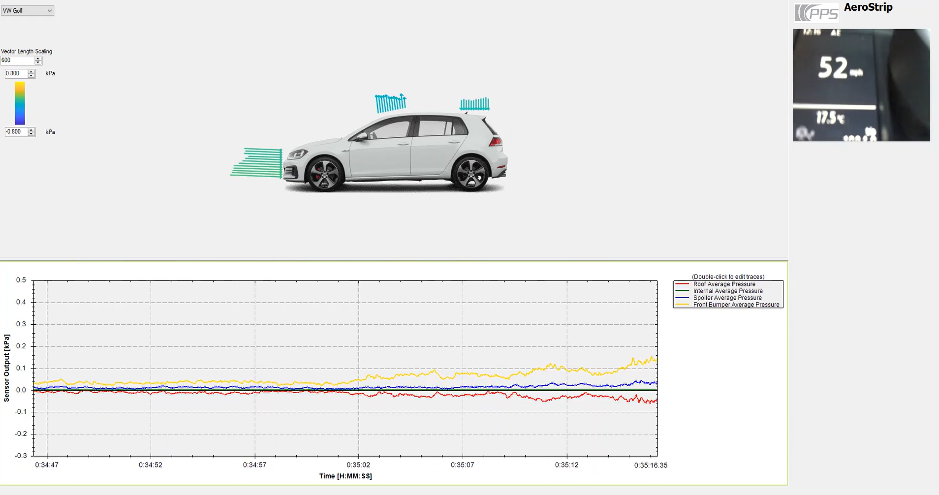
Aerodynamics
PPS aerodynamic sensing solutions, such as conformable pressure strips, enable surface pressure measurement without the complexity of traditional wind tunnel instrumentation. Lightweight and flexible, these AeroStrip sensors can be applied directly to curved or moving surfaces.
They provide high-resolution pressure distribution data for airflow analysis, CFD validation, and aerodynamic optimisation in real-world conditions.
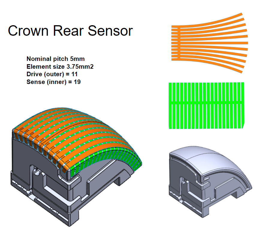
맞춤형 시스템 제작 및 개발
Many applications require more than an off-the-shelf solution. PPS specialises in custom tactile sensor development, working closely with customers from early concept through integration and validation.
Sensors can be tailored in geometry, pressure range, resolution, and electronics to meet specific mechanical and system-level requirements.
Key benefits
Bespoke sensor designs and layouts
Mechanical, electrical, and software integration support
Scalable solutions from prototype to production